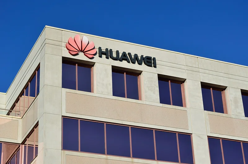
Huawei Technologies announced a strategic timeline to produce industry-leading semiconductors within the next five years using an unconventional technology framework. The initiative underscores Beijing’s broader efforts to neutralize stringent U.S. trade sanctions that have historically blocked China’s access to cutting-edge silicon. Speaking at a semiconductor symposium in Shanghai, Huawei stated that its high-end chips will achieve a transistor density equivalent to 1.4-nanometer (nm) nodes by 2031, though the firm omitted independent performance verification data. The milestone is highly ambitious given that China’s verified domestic fabrication limit currently hovers around 7-nm, while the global frontier is expected to hit the 1.4-nm threshold near the end of the decade. Due to Washington cutting off supply lines for advanced lithography machinery, market experts generally consider China unable to achieve these dimensions through traditional manufacturing tracks alone. For comparison, Taiwan’s TSMC currently manufactures at a 2-nm node and plans to initiate commercial 1.4-nm mass production by 2028.
To bypass these manufacturing bottlenecks, Huawei introduced an architectural philosophy dubbed the “Tau Scaling Law.” The principle acknowledges the limitations of Moore’s Law, noting that continuing to shrink transistors is hitting a physical wall where features are measured by just a few atoms. Instead of focusing entirely on transistor size, Huawei’s approach prioritizes reducing the transit time for signals and data moving across chips and computing architectures. While global chipmakers are universally exploring post-Moore’s Law concepts like advanced packaging and chiplets, the transition carries immense urgency for China. U.S. export controls have structurally locked Chinese tech firms out of the advanced tools required for leading-edge node fabrication, making alternative performance pathways essential to Beijing’s goal of semiconductor self-reliance. Industry analysts at Omdia view this as a credible strategic pivot from traditional node scaling to system-level efficiency, extracting higher performance through shortened interconnects and minimized latency rather than relying solely on finer lithography.
The geopolitical and economic stakes of this technological shift are heightened by the ongoing artificial intelligence boom. Huawei’s Ascend hardware line serves as the backbone for China’s premier domestic AI models, including DeepSeek’s recently launched flagship V4 framework. To commercialize its new architecture, Huawei revealed that its upcoming Kirin smartphone processors, slated for release later this year, will be the first to integrate a Tau Scaling design called “LogicFolding.” This design is engineered to condense internal chip wiring to boost overall performance. Huawei plans to scale LogicFolding into its Ascend AI processors by 2030, eventually deploying it across massive data center AI clusters. Over the past six years, the company’s silicon division has reportedly developed and mass-produced 381 chips using various iterations of Tau Scaling for mobile and enterprise applications.
Huawei’s focus on domestic architecture stems from its 2019 placement on a U.S. trade blacklist, which severed its access to American software, components, and global contract foundries. In response to what executives called an “extreme survival mode,” a highly classified internal backup plan led by He Tingbo, president of Huawei’s chip unit, became the cornerstone of the company’s resilience. The firm surprised the tech sector in 2023 by launching its 5G-capable Mate 60 smartphone series, which utilized a 7-nm system-on-chip manufactured domestically by Semiconductor Manufacturing International Corp (SMIC). Following Huawei’s recent LogicFolding announcement, SMIC shares climbed 7.6%, reflecting the market’s optimism; SMIC has also widened its post-Moore’s Law focus by establishing an advanced packaging research hub in Shanghai. Concurrently, domestic demand for Huawei’s Ascend processors has surged as Chinese tech giants seek alternatives to Nvidia, whose top-tier AI silicon remains restricted by U.S. export laws. Nvidia CEO Jensen Huang noted earlier this month that his company has largely conceded the Chinese AI chip landscape to Huawei.
Despite these notable architectural milestones, research analysts maintain that China still faces a competitive gap compared to international market leaders. Entities like Counterpoint Research note that managing cost, thermal output, power consumption, and hardware integration remains a formidable barrier, particularly for cloud-based AI infrastructure. While the strategic pivot may narrow near-term performance differentials, a structural gap regarding raw node fabrication persists. Huawei’s leadership openly acknowledged these hurdles, citing the immediate need for entirely new electronic design automation (EDA) tools optimized for Tau Scaling, alongside the ongoing challenge of mitigating heat dissipation across both mobile chips and massive data center deployments. However, the firm expressed confidence that its adapted solutions would keep its mobile and AI computing pipelines globally competitive over the next decade.
Click here for more on Technology